
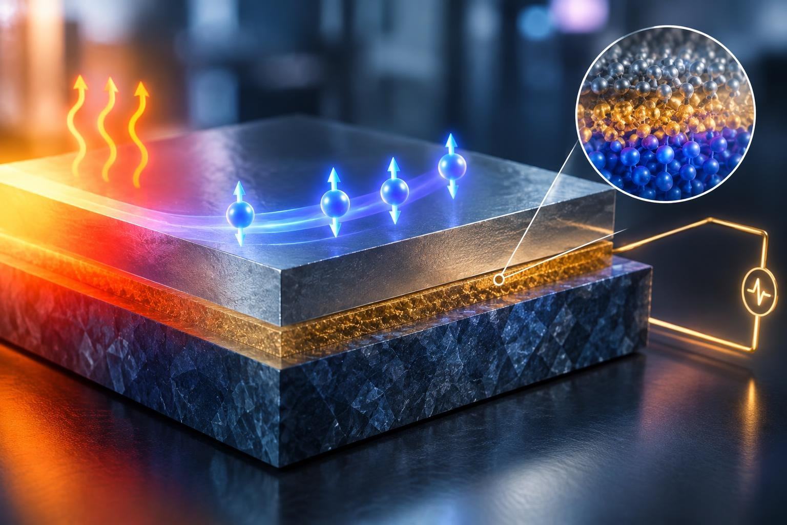
In conventional electronics, information is carried by moving electrical charge. Spintronics adds another property of electrons to the mix: their spin, a quantum feature that can be used to carry and process information. A new experiment suggests that a layer of metal thinner than a nanometer could help spin-based signals cross a crucial boundary more effectively.
Researchers at Kyushu University placed ultrathin iridium manganese, or IrMn, between a magnetic insulator and platinum. In their tests, a layer about 0.3 nanometers thick produced the strongest responses in two different spin-related effects. The result offers insight into how materials at an interface can influence spin transfer—a challenge for technologies that aim to use spin for computing or to turn waste heat into electricity.
Two ways to detect a spin current
The team’s structure combined yttrium iron garnet (YIG), a magnetic insulator, with platinum, a metal that can convert spin currents into measurable electrical signals. The researchers varied the thickness of the IrMn layer between them, from none to one nanometer, then measured two effects: the spin Seebeck effect and spin Hall magnetoresistance.
The spin Seebeck effect, or SSE, begins with a temperature difference across a magnetic material. That difference can generate a spin current—a flow of spin information rather than the ordinary flow of electrical charge. Platinum can turn that signal into a voltage, making the effect interesting for recovering some energy from heat that might otherwise be wasted.
Spin Hall magnetoresistance, or SMR, offers a different kind of readout. A metal’s electrical resistance changes depending on the orientation of its electrical current relative to the magnetization of a neighboring magnetic material. Studying SSE and SMR together let the researchers compare how spin is sent from YIG and how it is absorbed at the boundary.
Why a fraction of a nanometer matters
Spin signals can weaken as they pass through materials, so the boundaries between layers matter. One useful measure is spin mixing conductance: a description of how efficiently spin crosses the interface between magnetic and nonmagnetic materials. Earlier research had found that ultrathin inserted layers could improve spin-related signals, but the reasons were not fully clear.
In the Kyushu University experiments, the 0.3-nanometer IrMn sample gave the strongest SSE voltage and SMR response. The researchers also calculated spin mixing conductance from both measurements and found that the values agreed well. That consistency supports the idea that IrMn improves spin pumping and spin absorption through related interfacial processes.
At this thickness, IrMn is expected to form island-like patches rather than a smooth, continuous film. Those patches may affect how spin moves across the interfaces, but that explanation remains a possibility, not a settled finding. The team says further work is needed to separate the contributions of the individual interfaces.
Promising groundwork, not a finished device
The practical appeal is clear: if spin currents can be generated and detected more effectively, researchers may be able to build devices that do more with less electrical power. One possibility is using the spin Seebeck effect to power low-energy information devices from heat, potentially reducing reliance on batteries or an external power supply.
That is a prospective application, not something demonstrated by this experiment. The study examined a carefully designed material structure; it did not show a working battery-free product or establish how much usable energy a device could deliver. Turning an improved laboratory signal into useful computing or energy harvesting will require further engineering.
Still, the striking lesson is that the route for a spin signal may depend on a layer so thin it is not even continuous. In electronics, progress often comes from adding more power or more components. Here, the opportunity may lie in shaping the boundary—one tiny island of metal at a time.